Dalian Eastern Display Co., Ltd.
Dalian Eastern Display Co., Ltd.

This comprehensive guide delves into the intricacies of 0.42-inch OLED factory operations, exploring the manufacturing process, key players, technological advancements, and market trends. We'll examine the challenges and opportunities within this specialized sector, providing insights for those interested in understanding the production of these miniature displays.
The creation of a 0.42-inch OLED display begins with meticulous substrate preparation. This involves cleaning and treating the glass or plastic substrate to ensure optimal adhesion for subsequent layers. The organic materials that create the emissive pixels are then deposited using various techniques such as vacuum thermal evaporation or inkjet printing. The precise control of these processes is critical to achieving high-quality displays with consistent color and brightness.
Once the organic layers are deposited, the individual pixels are defined through photolithography or other patterning techniques. A crucial step is the encapsulation of the OLED structure, protecting it from moisture and oxygen, which degrade its performance and lifespan. This encapsulation often involves the use of barrier layers and sealing techniques.
The OLED layer is then integrated with a backplane, typically a thin-film transistor (TFT) array, which controls the individual pixels. Rigorous testing is performed throughout the process to ensure that the displays meet stringent quality standards. This includes testing for brightness, color accuracy, contrast ratio, and viewing angles. Advanced automated systems often handle much of the testing procedure.
While a complete list of all 0.42-inch OLED factory operators would be extensive, it's worth noting that many manufacturers specialize in smaller display sizes. These factories often cater to niche markets like wearable devices, smartwatches, and medical equipment. Detailed information on specific manufacturers is often proprietary, but researching industry reports can offer valuable insights.
Continuous innovation drives improvements in 0.42-inch OLED production. Researchers are constantly exploring new materials, processes, and techniques to enhance efficiency, reduce costs, and improve display performance. For example, advances in inkjet printing technology offer the potential for greater flexibility and lower production costs compared to traditional methods. Furthermore, the development of new, more efficient OLED materials contributes to increased brightness and longer lifespans.
The demand for small, high-quality displays is increasing as miniature electronics become increasingly sophisticated. The 0.42-inch OLED market is expected to experience continued growth, driven by applications in wearables, Internet of Things (IoT) devices, and medical instruments. However, challenges remain in terms of cost and production efficiency, particularly concerning the intricate manufacturing processes involved.
For more in-depth information on OLED technology and manufacturing, you can explore resources from industry associations and research institutions. Many academic papers and industry publications offer detailed analyses of OLED production methods and market trends.
| Aspect | Considerations for 0.42-inch OLED Production |
|---|---|
| Yield Rate | Maintaining high yield is crucial for cost-effectiveness, requiring precise process control and advanced quality assurance. |
| Defect Reduction | Minimizing defects through improved materials and processes is paramount to producing high-quality displays. |
| Cost Optimization | Balancing material costs, manufacturing efficiency, and equipment investment is essential for profitability. |
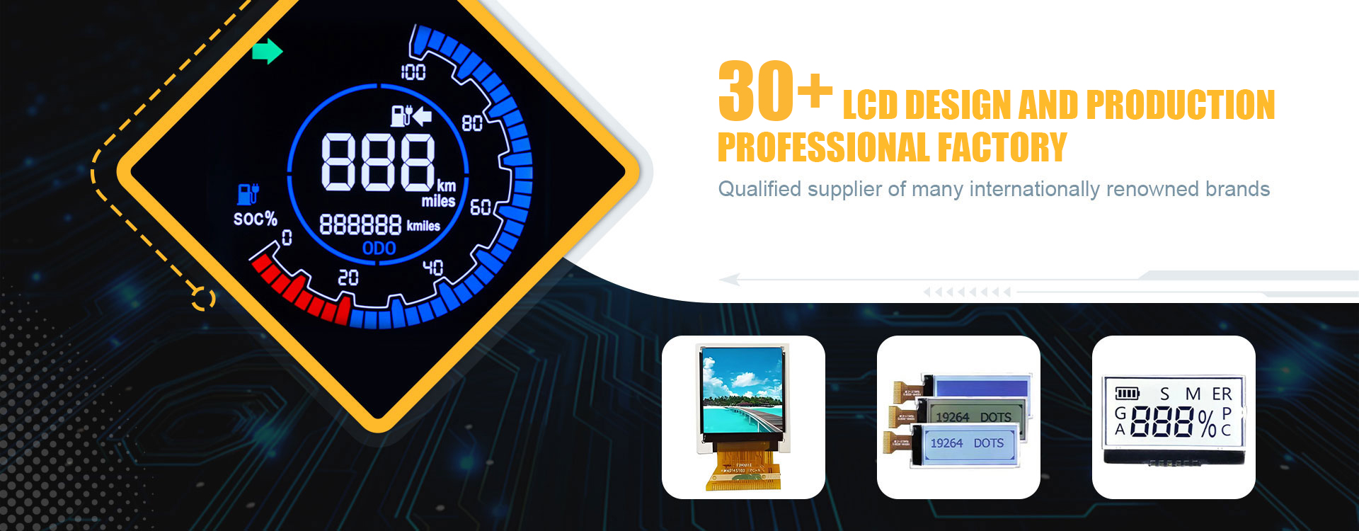
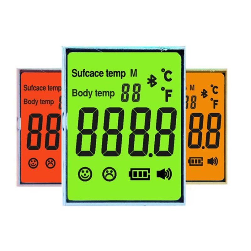
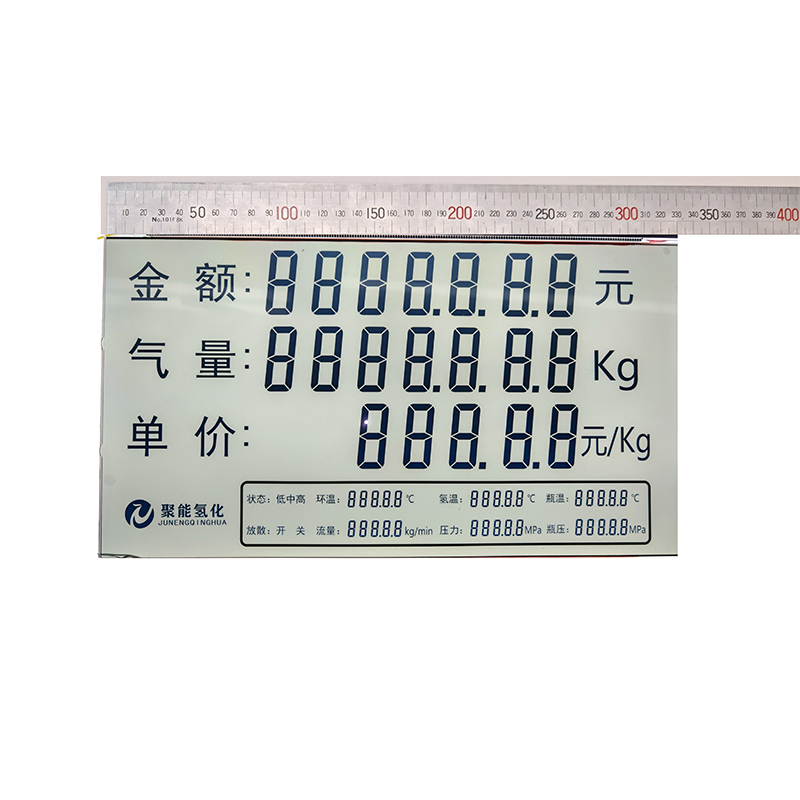
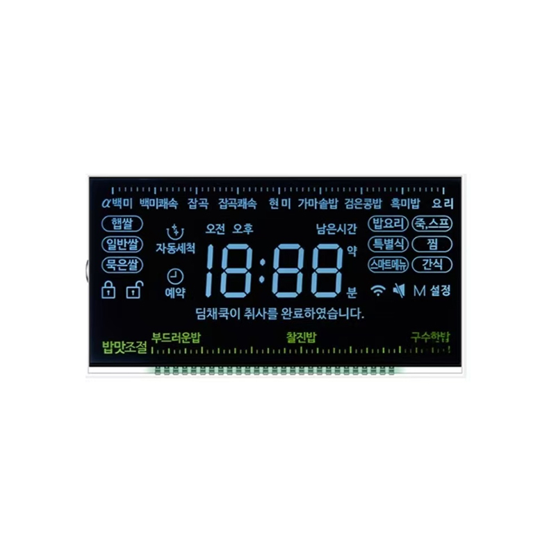
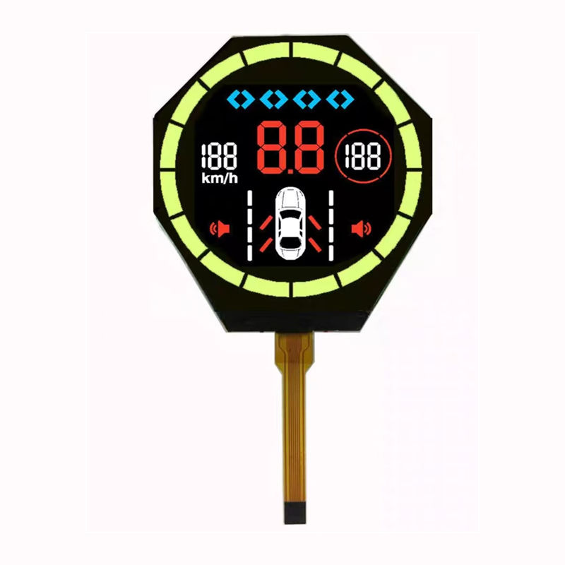
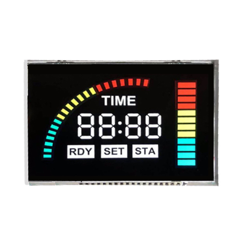
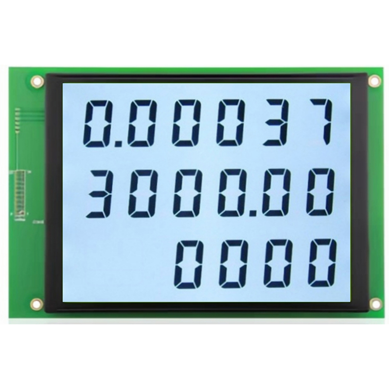
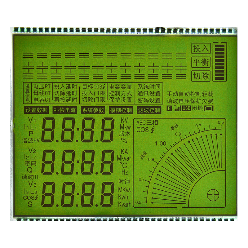
To learn more about high-quality LCD and OLED display solutions, explore the offerings of Dalian Eastern Display Co., Ltd. They are a leading provider of advanced display technologies.