Dalian Eastern Display Co., Ltd.
Dalian Eastern Display Co., Ltd.

This guide explores the intricacies of implementing the best FPGA SPI interface, covering various aspects from choosing the right configuration to optimizing performance. We'll delve into different approaches, highlight common pitfalls, and provide practical advice for achieving reliable and high-speed data transfer. Learn how to select the optimal SPI mode, manage clock synchronization, and handle potential error conditions. This comprehensive resource is designed for engineers of all levels seeking to master FPGA SPI interface design.
The Serial Peripheral Interface (SPI) bus is a synchronous, full-duplex communication protocol widely used in embedded systems for connecting microcontrollers and peripherals. Its simplicity and efficiency make it a popular choice for interfacing with various devices, including sensors, memory chips, and display controllers. An FPGA SPI interface offers the flexibility to customize the communication parameters to meet specific application requirements.
SPI operates in several modes, determined by the clock polarity (CPOL) and clock phase (CPHA). Understanding these configurations is crucial for establishing successful communication. Incorrect configuration can lead to data corruption. We'll examine each mode in detail, providing clear examples and practical considerations for choosing the best mode for your FPGA SPI interface.
Implementing an FPGA SPI interface involves assigning dedicated I/O pins for the MOSI, MISO, SCK, and SS lines. The choice of FPGA fabric resources (logic elements, block RAM, etc.) will depend on the desired throughput and complexity of the interface. We'll explore different architectures, including those leveraging built-in SPI peripherals or custom designs for maximum flexibility and performance. Consider using advanced features offered by your chosen FPGA to improve efficiency. For example, many FPGAs incorporate dedicated hardware blocks specifically designed for high-speed serial communication.
Efficient software design is equally crucial. The code responsible for controlling the FPGA SPI interface should handle data transfer, clock synchronization, and error detection. We'll present examples of VHDL and Verilog code snippets illustrating best practices. Proper error handling is critical for ensuring data integrity, so we will explore various methods of checking for errors and implementing appropriate recovery mechanisms.
Precise clock synchronization is paramount for reliable communication. We'll discuss methods for achieving stable clocking between the FPGA and the external SPI device. This often involves carefully considering clock domain crossing techniques to avoid metastability issues.
The data rate achievable with your FPGA SPI interface will depend on factors such as FPGA clock frequency, SPI mode, and the capabilities of the connected peripheral. Optimization strategies involve choosing appropriate SPI modes, efficiently managing data buffers, and leveraging FPGA resources to maximize throughput.
Data corruption can stem from various sources, including clock synchronization problems, incorrect SPI mode configuration, and noise on the communication lines. Effective error handling is essential. We'll outline strategies for detecting and correcting data errors. Implementing robust error detection and correction mechanisms helps maintain data integrity.
Different SPI devices may have different configurations and requirements. We'll address the challenges of interfacing with a variety of SPI peripherals and discuss how to adapt your FPGA SPI interface design to accommodate these differences.
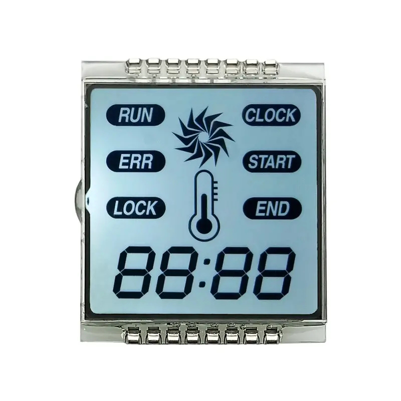
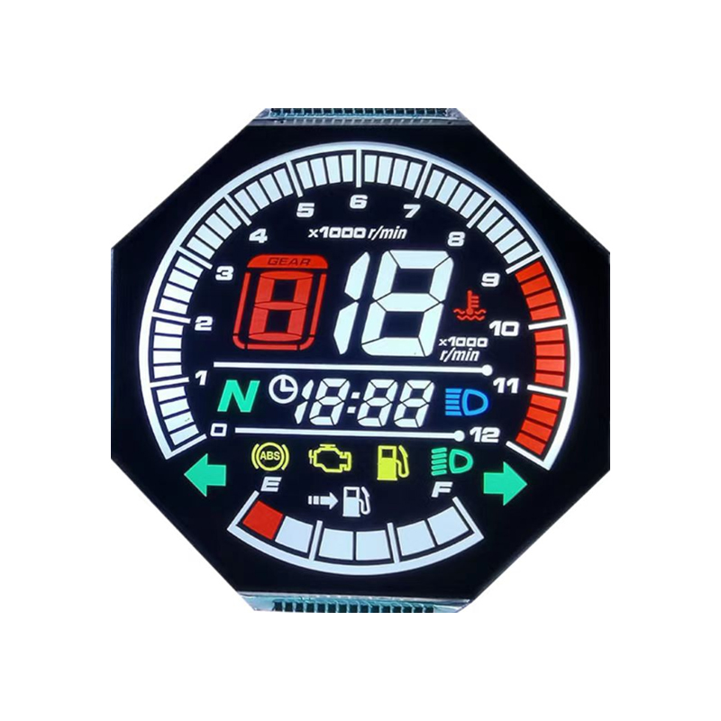
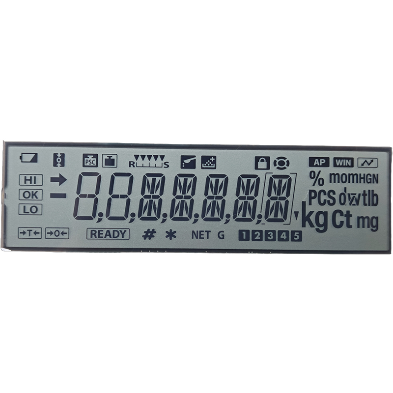
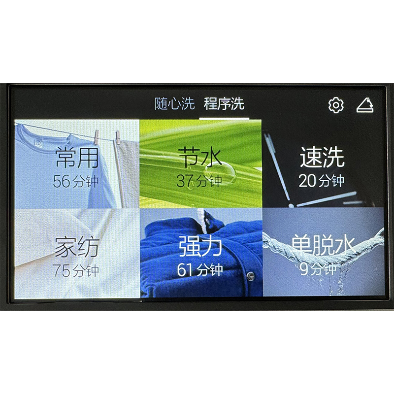
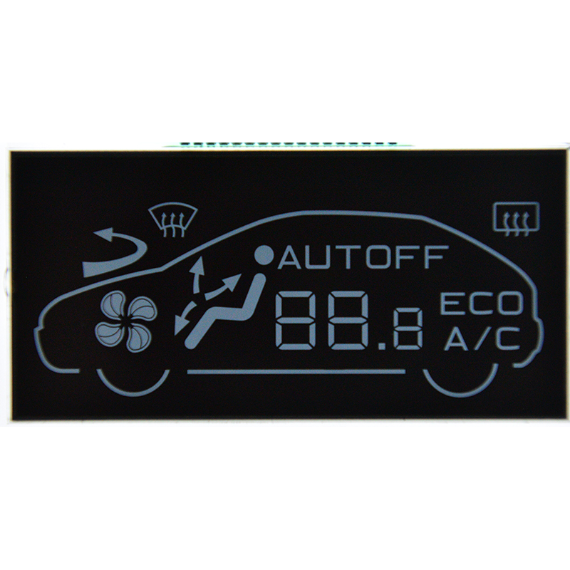
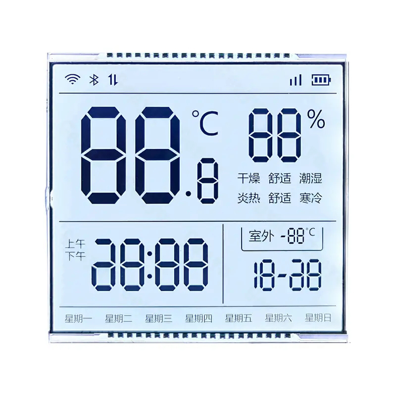
Mastering the FPGA SPI interface requires a thorough understanding of the SPI protocol, careful hardware design, and efficient software implementation. By following the guidelines and best practices outlined in this guide, you can create a robust and high-performance FPGA SPI interface for your embedded systems projects. Remember to always consult the datasheets of your specific FPGA and SPI peripherals for detailed specifications and recommendations. For high-quality LCD displays to integrate with your FPGA projects, consider exploring the options available at Dalian Eastern Display Co., Ltd. They offer a wide range of displays suitable for diverse applications.