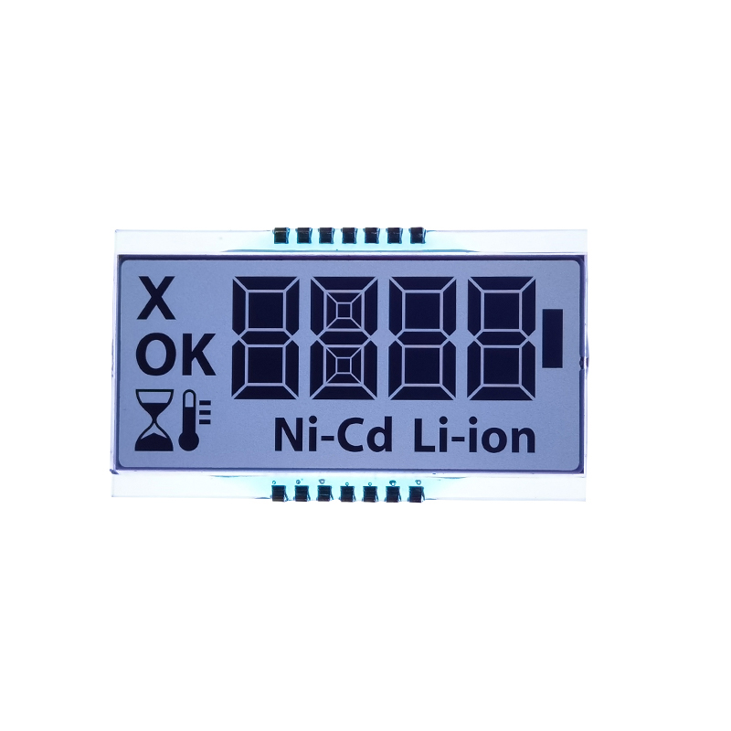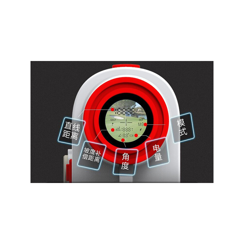
Dalian Eastern Display Co., Ltd.
Dalian Eastern Display Co., Ltd.

Best FPGA SPI Interface Exit StrategiesThis article explores effective strategies for managing SPI interface exits in FPGA designs, focusing on best practices for reliable and efficient data transfer. We'll cover various techniques, addressing common challenges and providing practical examples to improve your FPGA projects.
The SPI (Serial Peripheral Interface) bus is a widely used synchronous serial communication interface in embedded systems. Efficiently managing the exit from an SPI transaction is crucial for data integrity and overall system performance. Poorly handled exits can lead to data corruption, timing issues, and system instability. This guide examines several methods for achieving a clean and reliable Best FPGA SPI interface exit, considering factors such as clock synchronization, data buffering, and error handling.
One major challenge is preventing data corruption during the exit phase. Incomplete data transfers or premature termination can result in corrupted data being written to memory or used in subsequent computations. Robust error detection and correction mechanisms are essential to mitigate this risk.
Precise timing control is critical for a successful SPI transaction. The exit strategy must ensure that all data is transmitted and received correctly before the interface is released. Improper timing can lead to data loss or incorrect interpretation of data.
Efficient resource management is important, especially in resource-constrained FPGAs. The exit strategy should minimize the use of resources like registers, buffers, and logic elements, without compromising reliability. Careful planning and optimization can help conserve valuable resources.
Implementing dedicated signals to explicitly signal the end of the SPI transaction offers a clear and reliable mechanism. These signals can trigger cleanup routines and ensure all necessary steps are completed before the interface is deactivated. This is a common and effective strategy for a Best FPGA SPI interface exit.
Data buffers can help manage asynchronous data transfers. By buffering the data before and after the SPI transaction, we can ensure data integrity and decouple the SPI interface from the rest of the system. This technique is particularly valuable for high-speed SPI interfaces where timing is critical. Careful selection of buffer size is vital for balancing efficiency with potential memory constraints.
Error detection mechanisms, such as parity bits or CRC (Cyclic Redundancy Check), can detect data corruption during transmission. Error correction techniques can recover from some errors, improving the overall reliability of the SPI communication. The choice of error detection and correction method depends on factors such as the required reliability level and the available resources.
Using a state machine to manage the SPI interface exit provides a structured and controlled approach. This ensures that all necessary steps are performed in the correct order, minimizing the risk of errors. State machines can effectively manage complex interactions and timing requirements, contributing to a Best FPGA SPI interface exit implementation.
(This section would contain a detailed VHDL code example demonstrating a robust SPI exit strategy. Due to the complexity of providing a complete and accurate VHDL example within this response, it's omitted. However, numerous online resources and VHDL tutorials are readily available for guidance.)
The optimal strategy for a Best FPGA SPI interface exit depends on several factors, including the specific application, the speed of the SPI interface, and resource constraints. Carefully consider the trade-offs between different approaches before selecting the most suitable method for your project.
For further information on efficient embedded system design, consider exploring resources available from reputable FPGA manufacturers like Xilinx and Intel (Altera). Remember to always consult the official documentation for your specific FPGA device and SPI peripherals.