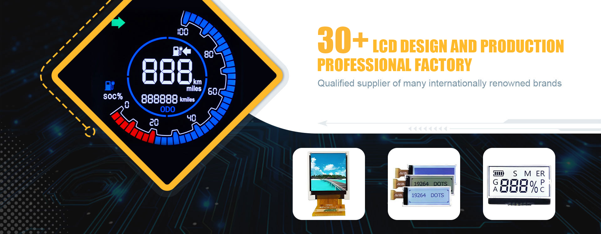
Dalian Eastern Display Co., Ltd.
Dalian Eastern Display Co., Ltd.

This guide provides a comprehensive overview of the Serial Peripheral Interface (SPI) and its implementation on Field-Programmable Gate Arrays (FPGAs). We'll cover the fundamentals of SPI communication, explore different design approaches for FPGA-based SPI interfaces, and delve into practical examples and troubleshooting tips. Learn how to efficiently integrate SPI peripherals into your FPGA projects and optimize performance for various applications.
The SPI bus is a synchronous, full-duplex serial communication interface widely used for short-distance communication. It utilizes four main signals: MOSI (Master Out Slave In), MISO (Master In Slave Out), SCK (Serial Clock), and SS/CS (Slave Select/Chip Select). Understanding the roles of each signal is crucial for successful FPGA SPI interface implementation. Data is transmitted bit by bit, with the clock signal synchronizing the data transfer. The Slave Select line is used to select a specific slave device on the bus. Different SPI modes exist, defined by the clock polarity (CPOL) and phase (CPHA) settings, influencing how data is sampled on the clock edge.
There are four main SPI modes (mode 0 to mode 3) determined by the CPOL and CPHA settings. These settings affect when data is sampled during the clock cycle. Choosing the correct mode is essential for communication with specific SPI peripherals. Incorrect mode selection will result in incorrect data transfer. The table below outlines the different modes:
| Mode | CPOL | CPHA | Description |
|---|---|---|---|
| Mode 0 | 0 | 0 | Idle clock is low, data is sampled on rising edge. |
| Mode 1 | 0 | 1 | Idle clock is low, data is sampled on falling edge. |
| Mode 2 | 1 | 0 | Idle clock is high, data is sampled on rising edge. |
| Mode 3 | 1 | 1 | Idle clock is high, data is sampled on falling edge. |
Implementing an FPGA SPI interface involves designing a module that interacts with the SPI peripherals. This typically involves using the FPGA's built-in logic blocks to create a state machine that manages the SPI communication protocol. Consider using IP cores provided by your FPGA vendor for simplified design and optimized performance. These cores often provide features such as DMA support for high-speed data transfer.
The design will be implemented using either Verilog or VHDL, depending on your preference and the tools you are using. The code will manage the four SPI signals and handle the data transfer based on the chosen SPI mode. A well-structured state machine is crucial for handling different phases of the communication, such as chip select assertion, data transmission, and chip select deassertion. Error handling and robust design are essential to ensure reliable communication.
For high-speed data transfer, consider techniques like using multiple SPI interfaces or employing advanced features offered by your FPGA such as dedicated high-speed serial interfaces or DMA controllers. Careful consideration of signal integrity is also crucial at higher frequencies to avoid signal distortion and data errors.
Supporting multiple SPI slaves requires managing multiple Slave Select lines. This can be achieved through a multiplexer or by assigning separate SPI instances to each slave. Properly managing the Slave Select signals is essential to avoid conflicts between multiple slave devices.
Debugging FPGA SPI interface issues can be challenging. Utilizing logic analyzers and debugging tools provided by your FPGA development environment are invaluable. Always verify your SPI mode settings, clock frequencies, and signal integrity to ensure proper communication. Following best practices for digital design, such as clear signal naming conventions and modular design, greatly improves the maintainability and debuggability of your project.
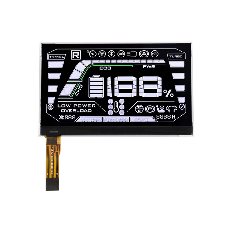
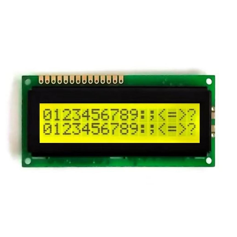
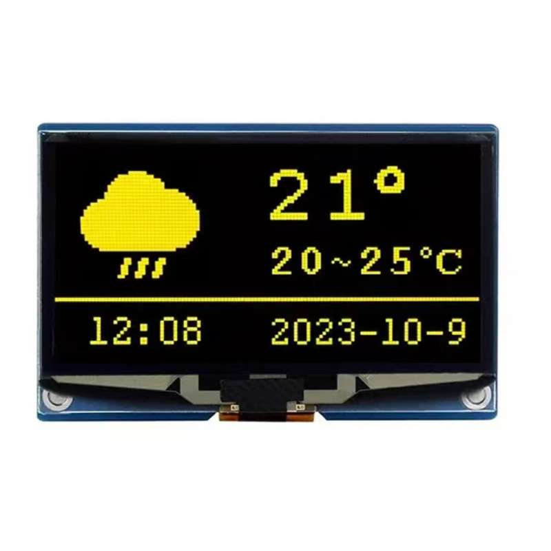
For more information on LCD displays and related technologies, you might find the resources at Dalian Eastern Display Co., Ltd. helpful. They offer a wide range of display solutions that often utilize SPI communication.
References:
1 [Add your reference here if you used any external sources]